MORE ON MEMORY DEVICES
Writing NOR Flash Driver
In this section I have discussed about the NOR Flash Commands and the operations supported by a “Generic NOR Flash Driver”. I have also provide a “Flash Driver example code in C” for “AT29LV040A Flash Memory”. This code can be used for any other Flash Memory, with minimum changes.
Intended Audience:
I have assumed that readers of this tutorial are familiar with the basic operation of a Static RAM. Familiarity with “C Programming Language” is also assumed. This tutorial and the accompanying example code could be of use to the beginners, who are just learning to interact with the NOR flash devices.
Flash Device Selection
Flash Manufacturer offer a wide range of Flash Devices with differing characteristics:
* Memory Size: Refers to the total Storage capacity (generally measured in terms of Mbits) of the memory device.
* Data Bus-width: This should be compatible with the data bus-width of processor, with which you are going to interface the Memory Device. Common bus widths are 8-bit and 16-bit.
* Programming speed: Time required to write a block of data in to Flash Memory
* Sector Size: Sector is the minimum unit of memory, which needs to be updated for any write operation. Flash memory is arranged as sectors of of fixed size (of the order of 100s of Bytes). Any write or erase operation on the memory device is performed on sector basis. If a write has to be performed on any single (or multiple) byte of a sector, then the contents of entire sector will have to be re-written.
The final selection of the device for your system will depend on the system requirements (e.g how much memory is needed, what sector size is best, what programming time is acceptable) and device compatibility (e.g. bus-width) with the other devices in system.
Flash Hardware Interface
A Flash Interface consists of signals quite similar to the Static SRAM
Ay..A0:
Form the address-bus. These pins are connected to the Address Bus of the Processor.
!OE:
Is the “active-low” “Output-enable” signal. This signal must be asserted (Along with !CE) during the read operations. This signal is connected to the “!Read” signal of the processor.
!WE:
Is the “active-low” “Write-Enable” signal. This signal is should be asserted during any command operation (more on this later). This signal is connected to the “!Write” signal of the processor.
!CE:
Is the “active-low” “Chip-enable” signal. This signal must be asserted while performing any operating on the memory device. This signal is connected to the “!Chip Select” signal of the processor.
Flash Commands
Flash Memory consists of memory cells which can be read in a way similar to a Static RAM. However modifying the state of these cells requires special programming voltages. The Flash devices have an in-built circuitry which can generate these special programming voltages. This circuitry has a state machine, which can receive inputs via external interface (external pins of the Memory Device). In order to modify the contents of the Flash, user needs to send some specific commands (via Address Bus, Data Bus, !OE, !WE and !CE signals) to the state machine of Flash Device.
Waiting for the Command Completion
After a command has been issued to the Flash Device, the internal state machine takes some time to execute this command (command completion time). This time is fixed for a given device (and is generally of the order of few m-seconds). After issuing any command, the flash programming software must wait for command completion (before starting any other operation). There are various ways to implement this wait logic in the flash driver software:
* Wait for a fixed number of processor cycles: Time taken by a processor to issue an instruction is fixed (for fixed processor clock). Generally most processors supports an “NOP” (no operation) instruction. This instruction does nothing, but wait for a processor cycle. Thus inserting a few “NOP” instructions the driver code will tantamount to a wait loop. For example if the processor core is running at a clock speed of 100 MHz (10ns cycle time) and the command completion time is “20 ms”, then inserting 2000, NOP instructions should help. Generally such NOP instructions can be inserted by implementing an empty FOR Loop (while writing code in C or any similar programming language). The problem with this approach is that flash driver needs to be aware of the processor “clock cycle time” and Flash “command completion time”.
* Data Polling: Flash devices support a special feature, where reading a word from the memory (during the command execution phase of flash) will return “invert” of the “last written value” on a specific bit. The wait loop, can keep polling this particular data bit to ensure the completion of flash command.
* Toggle Bit: Flash devices support another feature, where the value of a particular bit will toggle for each consecutive read operation, during the command execution phase. This is the most easy way for implementing the “command completion wait loop” as the driver software need not be aware of the last written value to the flash.
More on Sector-Size:
Flash Technology requires content of entire sector to be changed, even if a single byte in given sector needs to be modified. Too big a sector size can thus result in programming efficiency. However reducing the sector-size adds to the memory cost. Hence a trade-off is needed between efficiency and cost. Sector sizes of a few KBytes (128 Byte and 256 Bytes are most common sizes) , are suitable for most applications.
Typical Flash Commands
Sector Unlock:
To provide extra-protection to the Flash Memory against falsely triggered writes (unitentional operations like electrical transients and unintentional instructions), Flash memory devices offer a Sector Lock. Before performing any operation on the sector (erase or write), the sector must be unlocked.
Sector Erase:
A sector needs to be erased before writing in to the Flash. Generally flash memory cells can be thought of as an array of electronic switches. The value stored (0 or 1) in a memory cell, depends on the ability of this switch to conduct (or not conduct). When a memory has been erased, all the switches will be in no-conduction state (reads “1″). Any memory cell can be then programmed (by the internal state machine) to conduct (this is done by using special programming voltages). Hence, writing to any flash sector, must be preceeded by a sector erase operation.Sector Program:
To write specific data to the memory cells.Device Identification:
(Most) Memory devices have a unique Manufacturer-ID and a unique Product-ID associate with them. A system can thus support multiple Flash Devices. Ater power-on, system software (this can be a part of POST) can read these IDs to identify the flash chip and then use a programming software (out of various available softwares) for corresponding device.Writing in to Flash:
In order to modify the contents of a Flash Devices, one needs to issue a series of commands operations on the device.
* Sector-Unlock
* Sector-Erase
* Sector-Program
* Wait for programming cycle completion
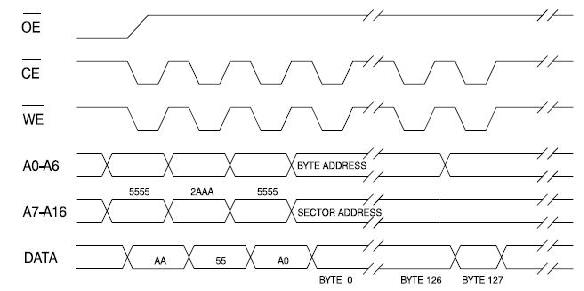
Fig. Flash Program Command for a 128-KByte memory with Sector Size of 128 Bytes
The AT29LV040A device
AT29LV040A offers 512KByte storage. The data bus width for this device is 8-bit and sector size is 256-Bytes. The device consists of 19 Address lines (A18..A0) to access the entire 512K words. Higher 11 MSBs of the address line identify a sector, and lower 8 address lines identify a word withing a sector.
(1) No sector unlock & Erase Operations: This memory device does not require any explicit “sector unlock” or “sector erase” function prior to “sector write). The internal state machine of the device, implement these functions by default, for any write operations. As we discussed before all the contents in a sector need to be re-written (because entire sector is erased prior to writing a single byte with in the sector).
(2) Block Lock Out command: The memory device is divided in to two memory blocks (upper and lower), each of 256 KBytes. Any of these blocks can be locked, by issuing a block lock out command. Once locked, the content of the block can not be modified (and there is no unlock command). Block lock is useful for storing the basic boot code in a system (e.g. boot loader). This ensures that system’s boot information will not be lost (modified or erased) because of some errors (e.g. system crash).
(3) Additional Chip Erase Command: The memory device provides an additional command which can erase the content of entire chip with a single command. If a memory block is locked out, it can not be erased.
Program Command
Program Command requires following sequence
* Load AA to address 5555
* Load 55 to address 2AAA
* load A0 to address 5555
* Load Data (entire 256 Bytes) for each byte of a sector
* wait for command completion (20ms, D7 is the poll bit and D6 is the toggle bit)
Block Lockout Command
* Load AA to address 5555
* Load 55 to address 2AAA
* Load 80 to address 5555
* Load AA to address 5555
* Load 55 to address 2AAA
* Load 40 to address 5555
* Load 00 to address 0000 (for locking lower block) OR Load FF to address 7FFFF (for locking higher block)
* Wait for command completion
Sotware Product Identification
In order to be able to read the Manufacturer-ID and Device-ID of the flash, user need to enter the product identification mode.
Entering the Product Identification mode:
* Load AA to address 5555
* Load 55 to address 2AAA
* Load 90 to address 5555
* wait for command completion
Exiting the Product Identification mode
* Load AA to address 5555
* Load 55 to address 2AAA
* Load F0 to address 5555
* wait for command completion
While in Product Identification mode
* A read from address 0×00000 will return the Manufacturer Id
* A read from address 0×00001 will return the Device Id
* A read from address 0×00002 will return FE (if no lock on lower block) or FF (if lock on lower block)
* A read from address 0×7FFF2 will return FE (if no lock on higher block) or FF (if lock on higher block)
Software Chip erase
* Load AA to address 5555
* Load 55 to address 2AAA
* Load 80 to address 5555
* Load AA to address 5555
* Load 55 to address 2AAA
* Load 10 to address 5555
* Wait for command completion
Timing Considerations:
In order for Flash Driver Software to function. it must be ensured that the electrical characteristics (voltage levels and signal timings) specified in the flash Memory Data sheet are satisfied. Please refer to the Device Data sheet for detailed timing informations and make sure the external memory interface on the processor (which is being used in your system) can meet these timings. Generally the memory signal timings from the processor are programmable using some control registers.
References:
(1) Atmel Flash Memory Overview
In previous section we discussed about NOR Flash Memories. In this section we will discuss about NAND Flash memories.
A NAND flash
is accessed in a way similar to block memory devices (e.g. Hard Disk, CF). The address and data lines on these devices are multiplexed, to reduce the pin count. Entire NAND flash is divided in to blocks, and each block is divided in to pages.NAND flash devices have higher memory density as compared to NOR flash devices. Their Programming life cycle is also higher. Cost is quite low. The design aim is to make the Flash memories cheaper, so that they can compete with other cheaper (e.g. Optical and Magnetic Memories) storage devices.
NAND flash Interface.
A typical NAND flash interface consists of following signals:
* I/O port: used for command, address, data
* Write enable: Should be asserted while writing commands, address or data.
* Read Enable: Should be enabled while reading the data.
* Address Latch Enable: Latches an Address from the I/O Bus
* Command Latch Enable: Latches a Command from I/O Bus
* Write Protect: When asserted, provide protection against inadvertent writes.
* Power Connections
* Other Control signals: e.g. CE
Samsung Chip K9F1208U0B
Samsung is pioneer in NAND flash technologies. In this section we will take example of K9F1208U0B and discuss different common operations on NAND flash memories.
This memory device is divided in to 4096 Blocks. Each block consists of 32 pages. Each page is 528 bytes (512 + 16). The memory device is divided in to four planes. Blocks 0, 4, 8 are on first plane. Blocks 1, 5, 9 form the second plane, and so on. The I/O Data port is byte wide.
ALE and CLE
The transfers on the NAND flash I/O interface could involve a command, data or address. The transfers are accordingly named as command phase, data phase and address phase. The combination of ALE and CLE identifies the current phase.
| ALE | CLE | Selection |
| 0 | 0 | Data |
| 1 | 0 | Address |
| 0 | 1 | Command |
| 1 | 1 | Not Defined |
Flash Operations
Any operation to be performed on a NAND device involves a command phase, followed by address phase (this phase is not needed for some operations), followed by data (input or output) phase.
* Command phase
Command phase is initiated by asserting the ~CS with "ALE=0" and "CLE=1". During the command phase the command word needs to be placed on the "I/O Port". Some command words may consists multiple bytes. In that case multiple command cycles are needed. Some common commands are read, program (write), erase, reset
* Address Phase
The memory device is accessed in form of rows and columns. A particular page (on any block) is identified by a unique row address. A column address identifies a particular byte with in a page. Page is divided in to two halves. First half and second half. A single bit is used to select one of these halves. A byte with in these halves can be identified using a unique 8-bit address. This reduces the column address to 8-bits. The address phase on I/O port involves multiple address cycles. The column address followed by row address is sent out on the I/O port during these multiple cycles.
* Data phase
Data phase involves data input (for program operation) to the Flash or data output (for read, status etc.) from the Flash, via I/O port. The ~WE signal needs to be asserted for writing in to the Flash, and ~RE signal needs to be asserted for reading from the Flash. Both ~WE and ~RE should not be asserted at same time.
Interfacing a CPU with NAND flash devices
Some processors come with an in-built NAND flash controller. The controller can generate control/data signals required for a NAND flash memory. Such processors have an external NAND flash interface which can be gluelessly interfaced to the industry standard NAND flash memories.
A processor which does not have an inbuilt NAND flash controller can use its parallel port (and some GPIO flags) to emulate the NAND flash interface.
Performance of K9F1208U0B
Program operation can be done in 200 us on a single page. Block erase in 2 ms on a single block. Data on a page can be read in 50ns cycle time per Byte. 100 K program/erase cycles are supported.
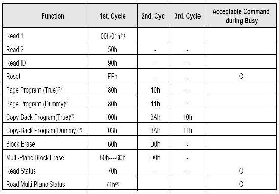
K9F1208U0B Command Set
Intended Audience
This tutorial covers basic of DRAM technology and its usage. This tutorial may be of use to the Embedded System Designers (Software and Hardware).
Introduction
DRAMs (Dynamic Random Access Memories) are increasingly becoming popular in embedded system domain. DRAMs store each bit of data on capacitor cells. Since a capacitor continuously leaks data, DRAMs need periodic refresh (recharging of capacitor to original value). This makes the DRAM hardware design more complicated than SRAMs (Static Random Access Memory). Any read of write to a Static RAM requires a single access. Accessing DRAM on the contrary involves a series of operations. DRAM access is therefore much slower than SRAM. However DRAM are increasingly becoming popular because of their higher memory density (more bits/area) and hence low-cost (less cost/bit). Each storage cell of SRAM is made up of six transistors. On the other hand DRAM uses a capacitor and a single transistor to store the charge. The cost advantage of DRAM outweighs the limitations. DRAMs are integral part of most modern embedded system.
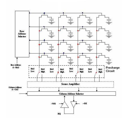
A DRAM Cell
A 1-bit DRAM cell consists of a capacitor and a transistor. A number of such cells are arranged as a rectangular matrix (in terms of rows and columns) to make a memory bank. A particular DRAM cells can be accessed with help of row-address and a column-address. Most modern devices consist of 4-bit, 8-bit or 16-bit cells (instead of a 1-bit cell). Figure below shows DRAM with 1-bit cells arranged in a 4×4 matrix forming 4-columns and 4 rows.
Row and Column Addresses
The DRAM cells are arranged as a rectangular matrix. Each cell can be accessed using a Row and Column Index (address). While addressing a particular cell, first corresponding row is enabled, and then the column with in this row is selected.
Capacitor Storage Cells
Capacitor in the above figure is used to store the charge.
Transistors
The transistors act like a switch. Selecting a particular row address and asserting the ~RAS signal will switch-on all the transistors in a given row. The switch outputs are connected to sense amplifiers.
Word Lines
The horizontal lines in given figure, which connect gates of all the transistors in a given row are called word lines.
Bit Lines
The vertical lines connecting switch outputs of a given column are called bit lines. There are two bit lines positive and negative. These bit lines are connected to sense amplifier circuitry.
Pre-charge circuit
A pre-charge circuit can pre-charge positive and negative bit lines to an initial voltage VDD/2.
Sense Amplifiers
Sense amplifiers are differential amplifiers. The bit lines (positive and negative) are input to the sense amplifiers. Sense amplifiers also have a provision for feeding the output back to bit lines.
Precharge command
Pre-charge command is used to pre-charge both the bit lines to VDD/2.
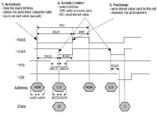
Row Activation
Row activation is performed by asserting the ~RAS and providing the row address of desired row. Asserting the ~RAS pre-charges both the bit lines to VDD/2 (with help of pre-charge circuit). In the mean time, the switch transistors for particular row start to conduct (switch turns on). This connects the capacitor cells to the positive bit lines. The potential on positive bit line changes (increases to VDD/2 + delta or decreases to VDD/2 - delta) based on the cell charge on capacitor. The voltage change on bit line is small because the cell capacitance is generally much smaller (generally fractions of pF) as compared to the capacitance of transistor and the bit line. Sense amplifier amplifies this small voltage difference to either VDD or Zero. The sense amplifier output gets latched (this latch has not been shown in the figure but it exists) and row activation is complete.
Column Read
Once the output from a given row is available at sense amplifiers, any of the columns can be read by enabling the Column Access (using ~CAS and column address) and ~OE. Reading multiple columns from same row is very easy. For accessing a cell from a different row, new row needs to be activated. Closing a row requires the cells of current row to be restored as we will discuss later.
Column Write
Column write involves forcing the bit lines to a desired voltage after row activation.
Row pre-charge
The reading operation discharges the capacitors cell of particular row. These capacitors need to be recharged after the read operation is over. This operation is called row pre-charge (do not confuse it with pre-charge command). The row pre-charge is not needed while performing successive read operations from the same row. When a read/write operation has to be performed from another row, the current row pre-charged.
Reading
* Row Activation
* Column Read
* Row pre-charge
Writing
* Row Activation
* Column Write
Row refresh
As we discussed before the capacitive storage cells leak charge. There is a need of periodically refreshing the rows. Row refresh involves row activation followed by row pre-charge (without enabling the ~OE or ~WE buffers). Generally the refresh period is of the order of few ms (64 ms being most common). There are two ways to implement auto-refresh. Either all the rows can be refreshed every 64ms. Or different rows can be periodically refreshed (one at a time) such that each row is refreshed every 64 ms. For example if there are 1024 rows, a row refresh can be performed every 62.5 us.
DRAM Variations
Asynchronous DRAM
This is the basic form, from which all others are derived.
Synchronous DRAM
SDRAM has a synchronous interface, meaning that it waits for a clock signal before responding to its control inputs. It is synchronized with the processor’s system bus. The clock is used to drive an internal state machine that pipelines incoming instructions. This allows the chip to have a more complex pattern of operation than asynchronous DRAM which does not have synchronizing control circuits. SDRAM can support burst mode accesses. SDRAM is also known as SDR SDRAM (single Data Rate SDRAM).
DDR SDRAM
DDR (Dual Data Rate) SDRAM achieves greater bandwidth than the preceding SDR SDRAM by transferring data on the rising and falling edges of the clock signal (double pumped). Effectively, it nearly doubles the transfer rate without increasing the frequency of the front side bus.
DRAM Interface
A SDRAM interface involves following common signals
~CAS
~RAS
~WE
~OE
Address Pins
Data Pins (bi-directional)
CLK and CLKEN (in case of SDRAM)
Power connections
DRAM Controller
Since the addressing scheme and read/write operations in an SDRAM are slightly different from that of an SRAM, these devices can not be directly interfaced to the processors which provide SRAM interface. A SDRAM controller needs to be used to control the operations of an SDRAM. Most modern processors have an in-built SDRAM controller. The SDRAM controller needs to be programmed with different parameters (like row size, column size, refresh period etc) before accesses to SDRAM can be made. The SDRAM parameters are dependent on SDRAM device being used.
Self refresh mode (for power down operations)
The Self-refresh mode can be used to retain data in the SDRAM, even if the rest of the system is powered down. An internal timer meets all the refresh requirements. This feature provides the capability to reduce power consumption during refresh operations. In self-refresh mode, the address buffer and command interface are disabled.
User Comments
No Posts found !Login to Post a Comment.