Microcontroller PIC16F84
Introduction
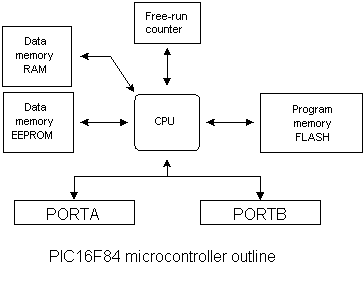
PIC16F84 belongs to a class of 8-bit microcontrollers of RISC architecture. Its general structure is shown on the following map representing basic blocks.
Program memory (FLASH)- for storing a written program.
Since memory made in FLASH technology can be programmed and cleared more than once, it makes this microcontroller suitable for device development.
EEPROM - data memory that needs to be saved when there is no supply.
It is usually used for storing important data that must not be lost if
power supply suddenly stops. For instance, one such data is an assigned temperature in temperature regulators. If during a loss of
power supply this data was lost, we would have to make the adjustment once again upon return of supply. Thus our device looses on self-reliance.
RAM - data memory used by a program during its execution.
In RAM are stored all inter-results or temporary data during run-time.
PORTA and PORTB are physical connections between the microcontroller and the outside world. Port A has five, and port B
has eight pins.
FREE-RUN TIMER is an 8-bit register inside a microcontroller that works independently of the program. On every fourth clock of the oscillator it increments its value until it reaches the maximum (255), and then it starts counting over again from zero. As we know the exact timing between each two increments of the timer contents, timer can be used for measuring time which is very useful with some devices.
CENTRAL PROCESSING UNIT has a role of connective element between other blocks in the microcontroller. It coordinates the work of other blocks and executes the user program.
CISC, RISC
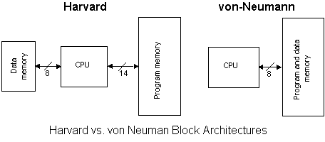
It has already been said that PIC16F84 has a RISC architecture. This term is often found in computer literature, and it needs to be explained here in more detail. Harvard architecture is a newer concept than von-Neumann's. It rose out of the need to speed up the work of a microcontroller. In Harvard architecture, data bus and address bus are separate. Thus a greater flow of data is possible through the central processing unit, and of course, a greater speed of work. Separating a program from data memory makes it further possible for instructions not to have to be 8-bit words. PIC16F84 uses 14 bits for instructions which allows for all instructions to be one word instructions. It is also typical for Harvard architecture to have fewer instructions than von-Neumann's, and to have instructions usually executed in one cycle.
Microcontrollers with Harvard architecture are also called "RISC microcontrollers". RISC stands for Reduced Instruction Set Computer. Microcontrollers with von-Neumann's architecture are called 'CISC microcontrollers'. Title CISC stands for Complex Instruction Set Computer.
Since PIC16F84 is a RISC microcontroller, that means that it has a reduced set of instructions, more precisely 35 instructions . (ex. Intel's and Motorola's microcontrollers have over hundred instructions) All of these instructions are executed in one cycle except for jump and branch instructions. According to what its maker says, PIC16F84 usually reaches results of 2:1 in code compression and 4:1 in speed in relation to other 8-bit microcontrollers in its class.
Applications
PIC16F84 perfectly fits many uses, from automotive industries and controlling home appliances to industrial instruments, remote sensors, electrical door locks and safety devices. It is also ideal for smart cards as well as for battery supplied devices because of its low consumption.
EEPROM memory makes it easier to apply microcontrollers to devices where permanent storage of various parameters is needed (codes for transmitters, motor speed, receiver frequencies, etc.). Low cost, low consumption, easy handling and flexibility make PIC16F84 applicable even in areas where microcontrollers had not previously been considered (example: timer functions, interface replacement in larger systems, coprocessor applications, etc.).
In System Programmability of this chip (along with using only two pins in data transfer) makes possible the flexibility of a product, after assembling and testing have been completed. This capability can be used to create assembly-line production, to store calibration data available only after final testing, or it can be used to improve programs on finished products.
Clock / instruction cycle
Clock is microcontroller's main starter, and is obtained from an external
component called an "oscillator". If we want to compare a microcontroller with a time clock, our "clock" would then be a ticking sound we hear from the time clock. In that case, oscillator could be compared to a spring that is wound so time clock can run. Also, force used to wind the time clock can be compared to an electrical supply.
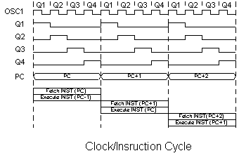
Clock from the oscillator enters a microcontroller via OSC1 pin where internal circuit of a microcontroller divides the clock into four even clocks Q1, Q2, Q3, and Q4 which do not
overlap. These four clocks make up one instruction cycle (also called machine cycle) during which one instruction is executed.
Execution of instruction starts by calling an instruction that is next in string. Instruction is called from program memory on every Q1 and is written in instruction register on Q4. Decoding and execution of instruction are done between the next Q1 and Q4 cycles. On the following diagram we can see the relationship between instruction cycle and clock of the oscillator (OSC1) as well as that of internal clocks Q1-Q4. Program counter (PC) holds information about the address of the next instruction.
Pipelining
Instruction cycle consists of cycles Q1, Q2, Q3 and Q4. Cycles of calling and executing instructions are connected in such a way that in order to make a call, one instruction cycle is needed, and one more is needed for decoding and execution. However, due to pipelining, each instruction is effectively executed in one cycle. If instruction causes a change on program counter, and PC doesn't point to the following but to some other address (which can be the case with jumps or with calling subprograms), two cycles are needed for executing an instruction. This is so because instruction must be processed again, but this time from the right address. Cycle of calling begins with Q1 clock, by writing into instruction register (IR). Decoding and executing begins with Q2, Q3 and Q4 clocks.
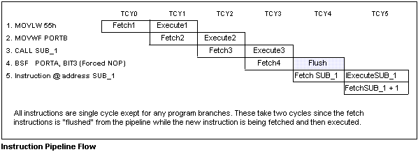
TCY0 reads in instruction MOVLW 55h (it doesn't matter to us what instruction was
executed, because there is no rectangle pictured on the bottom).
TCY1 executes instruction MOVLW 55h and reads in MOVWF PORTB.
TCY2 executes MOVWF PORTB and reads in CALL SUB_1.
TCY3 executes a call of a subprogram CALL SUB_1, and reads in instruction BSF PORTA, BIT3. As this instruction is not the one we need, or is not the first instruction of a subprogram SUB_1 whose execution is next in order, instruction must be read in again. This is a good example of an instruction needing more than one cycle.
TCY4 instruction cycle is totally used up for reading in the first instruction from a subprogram at address SUB_1.
TCY5 executes the first instruction from a subprogram SUB_1 and reads in the next one.
Pin description
PIC16F84 has a total of 18 pins. It is most frequently found in a DIP18 type of case but can also be found in SMD case which is smaller from a DIP. DIP is an abbreviation for Dual In Package. SMD is an abbreviation for Surface Mount Devices suggesting that holes for pins to go through when mounting, aren't necessary in soldering this type of a component.
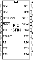
Pins on PIC16F84 microcontroller have the following meaning:
Pin no.1 RA2 Second pin on port A. Has no additional function
Pin no.2 RA3 Third pin on port A. Has no additional function.
Pin no.3 RA4 Fourth pin on port A. TOCK1 which functions as a timer is also found on this pin
Pin no.4 MCLR Reset input and Vpp programming voltage of a microcontroller
Pin no.5 Vss Ground of power supply.
Pin no.6 RB0 Zero pin on port B. Interrupt input is an additional function.
Pin no.7 RB1 First pin on port B. No additional function.
Pin no.8 RB2 Second pin on port B. No additional function.
Pin no.9 RB3 Third pin on port B. No additional function.
Pin no.10 RB4 Fourth pin on port B. No additional function.
Pin no.11 RB5 Fifth pin on port B. No additional function.
Pin no.12 RB6 Sixth pin on port B. 'Clock' line in program mode.
Pin no.13 RB7 Seventh pin on port B. 'Data' line in program mode.
Pin no.14 Vdd Positive power supply pole.
Pin no.15 OSC2 Pin assigned for connecting with an oscillator
Pin no.16 OSC1 Pin assigned for connecting with an oscillator
Pin no.17 RA2 Second pin on port A. No additional function
Pin no.18 RA1 First pin on port A. No additional function.
User Comments
No Posts found !Login to Post a Comment.