LM35 Based Temperature controller using PIC16F877a microcontroller
AIM:
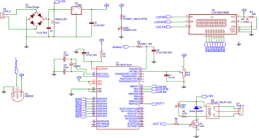
To design Temperature controller by using PIC16F877a microcontroller. It has 8 analog channel. In this project, 2 analog channel used to read temperature value from LM35 as well as set point value from a POT. The Temperature value and setpoint value will be displayed two row LCD display(2X16).
Circuit Diagram:

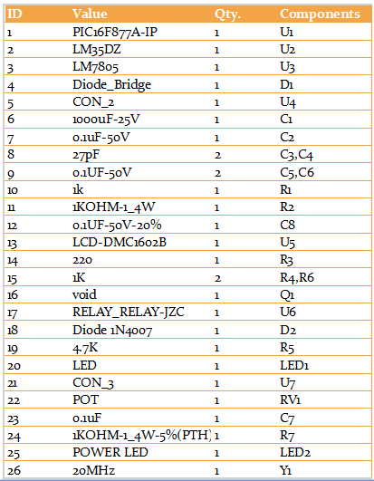
Parts Descriptions:

More details of circuit diagram and PCB Layout here.
Working Description:
Firmware code for PIC is developed in MPLAB IDE. LM35 used to sense Temperature. The LM35 series are precision integrated-circuit temperature devices with an output voltage linearly-proportional to the Centigrade temperature. The LM35 device has an advantage over linear temperature sensors calibrated in Kelvin, as the user is not required to subtract a large constant voltage from the output to obtain convenient Centigrade scaling. The LM35 device does not require any external calibration or trimming to provide typical accuracy of ±¼°C at room temperature and ±¾°C over a full -55°C to 150°C temperature range.
The output of LM35 is given into analog channel of PIC16F877a microcontroller. A POT used to adjust the setpoint value. The main process of microcontroller is set the output according to the comparison of LM35 value and setpoint value. And also display these values in LCD.
Application:
1. Industrial motor safety protection.
2. Soldering iron protection.
3. Room Temperature control.
4. Temperature control in research labs.
Assembly source file:
			PROCESSOR PIC16F877A
			#INCLUDE

 __CONFIG _CP_ON & _WDT_OFF & _PWRTE_ON & _HS_OSC

			ORG 0X000
			GOTO MAIN
			ORG 0X004
			retfie


	CONSTANT BASE = 0x20		; base address of user file registers
	CONSTANT LCDWAIT = 0x20 	; clk in [0..5] MHz
	CONSTANT LCDTYPE = 0x00		; clk in [0..9] MHz

FLAGreg	equ	BASE+d'4'
#define	LCDbusy FLAGreg,0x00	; LCD busy flag declared within flag register
#define	LCDcflag FLAGreg,0x01


LCDtris	equ	TRISD		; LCD data on low nibble of portA
LCDport	equ	PORTD

#define	LCD_ENtris TRISB,0x02	; EN on portB,1
#define	LCD_EN     PORTB,0x02	; Enable Output / "CLK"
#define	LCD_RStris TRISB,0x00	; RS on portB,2
#define	LCD_RS     PORTB,0x00	; Register Select
#define	LCD_RWtris TRISB,0x01	; RW on portB,3
#define	LCD_RW     PORTB,0x01	; Read/Write

; Hardware Configuration

FOSC            equ     .20000000        ; 20Mhz crystal resonator
BITRATE         equ     .100000         ; 100KHz I2C speed


#DEFINE RLY PORTB,7
LM35_VAL        EQU 0X50
POT_VAL        EQU 0X51

DE1				EQU 0X60
DE2				EQU 0X61
DE3				EQU 0X62
TEM				EQU 0X63
TTTEM			EQU 0X64

; rx_math32.inc  ---------------------variables------------------------------//

REGA0			EQU 0X66				;lsb
REGA1			EQU 0X67
REGA2			EQU 0X68
REGA3			EQU 0X69				;msb

REGB0			EQU 0X6A				;lsb
REGB1			EQU 0X6B
REGB2			EQU 0X6C
REGB3			EQU 0X6D				;msb

REGC0			EQU 0X6E				;lsb
REGC1			EQU 0X6F
REGC2			EQU 0X70
REGC3			EQU 0X71				;msb

DSIGN			EQU 0X72				;Digit Sign. 0=positive,1=negative
DIGIT1			EQU 0X73				;MSD
DIGIT2			EQU 0X74
DIGIT3			EQU 0X75
DIGIT4			EQU 0X76
DIGIT5			EQU 0X77				;Decimal (BCD) digits
DIGIT6			EQU 0X78
DIGIT7			EQU 0X79
DIGIT8			EQU 0X7A
DIGIT9			EQU 0X7B
DIGIT10			EQU 0X7C	;LSD

MTEMP			EQU 0X7D
MCOUNT			EQU 0X7E
DCOUNT			EQU 0X7F

			#INCLUDE
			#INCLUDE
			#INCLUDE

MAIN
			BANKSEL TRISB
			MOVLW B'00011111'
			MOVWF TRISA
			MOVLW B'00001111'
			MOVWF TRISC
			MOVLW B'00000000'
			MOVWF TRISB
			MOVLW B'11000010'
    		MOVWF ADCON1
			MOVLW B'00000111'
			MOVWF TRISD
			BANKSEL PORTB
			MOVLW B'10000001'
    		MOVWF ADCON0
			CLRF INTCON
			movlw .3
			movwf DE3
			LCDinit
			CALL INITDIS

MAINN
			DECFSZ DE1,1
			B MAINN
			DECFSZ DE2,1
			B MAINN
			DECFSZ DE3,1
			B MAINN
			movlw .3
			movwf DE3
			B FETCH


INITDIS
			LCDline 1
			LCDPUTLine "Temperature:"
			LCDline 2
			LCDPUTLine "Set Value  :"
			RETURN

FETCH
			MOV32REG REGA0, d'100';        ; LM35 Route
			CALL GET_LM35
			CALL MULTIPLY
			MOV32REG REGB0, d'205';
			CALL DIVIDE
			movf REGA0,w
			MOVWF LM35_VAL
			call BIN2DEC
			LCD_DDAdr d'12'
			movf DIGIT8,w
			addlw .48
			LCDw
			movf DIGIT9,w
			addlw .48
			LCDw
			movf DIGIT10,w
			addlw .48
			LCDw
			movlw 'C'
			LCDw

			MOV32REG REGA0, d'100';        ; POT Route
			CALL GET_POT
			CALL MULTIPLY
			MOV32REG REGB0, d'1023';
			CALL DIVIDE
			movf REGA0,w
			MOVWF POT_VAL
			call BIN2DEC
			LCD_DDAdr d'76'
			movf DIGIT8,w
			addlw .48
			LCDw
			movf DIGIT9,w
			addlw .48
			LCDw
			movf DIGIT10,w
			addlw .48
			LCDw
			movlw 'C'
			LCDw

			MOVF LM35_VAL,0             ; Compare two value and set output
			SUBWF POT_VAL,w
			BTFSC STATUS,C
			BCF RLY
			BTFSS STATUS,C
			BSF RLY
			goto MAINN

GET_POT
			BSF ADCON0,3          ;Select POT ADC Channel
			b GETADC

GET_LM35
			BcF ADCON0,3          ;Select LM35 ADC Channel
GETADC
			movlw .250
			call BITDELAY
			BSF ADCON0,2
			BTFSC ADCON0,2
			B $-1
			nop
			nop
			clrf REGB3
			clrf REGB2
			movf ADRESH,w
			movwf REGB1
			BANKSEL ADRESL
			MOVF ADRESL,w
			BANKSEL PORTB
			MOVWF REGB0
			RETURN

BITDELAY                    ; TEM*150 microsecond delay
			MOVWF TEM
SSS1
			DECFSZ TTTEM,1
			GOTO SSS1
			DECFSZ TEM,1
			GOTO SSS1
			RETURN
	END
Include files here
User Comments
No Posts found !Login to Post a Comment.